Select a different country or region to see specific content for your location.
Back-End applications
Materials and Solutions for Back-End applications
Back-End applications
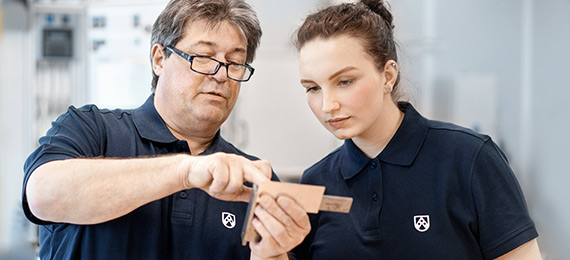
The further processing of IC-Chips in the back-end sector is a fundamentally important step in the production of reliable semiconductors. The back-end applications required for this include testing of the chips and cutting the wafers into single chips. Röchling therefore offers highly loadable materials to produce test sockets or material solutions, such as antistatic equipment, to optimize your dicing process.
![[Translate to Japanese:]](/fileadmin/_processed_/4/d/csm_Testsocket_1980x800_61da4a9ad8.jpg "[Translate to Japanese:]")
Arrange technical advice
The performance and service life of plastics for use in the semiconductor industry are influenced by a variety of factors. These criteria need to be considered in order to make the right choice in materials. Examples:
- Antistatic or conductive properties
- Operating temperature
- Contact with chemicals
- Design requirements
- Dimensions and tolerances
- Flame retardancy
We are happy to advise you on the selection of suitable materials for your particular application. Just use our contact form at the bottom of the page.