Select a different country or region to see specific content for your location.
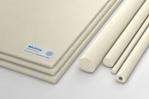
Materials and solutions for CMP
[Translate to Japanese:] Materials and solutions for Chemical Mechanical Planarization (CMP)
[Translate to Japanese:]
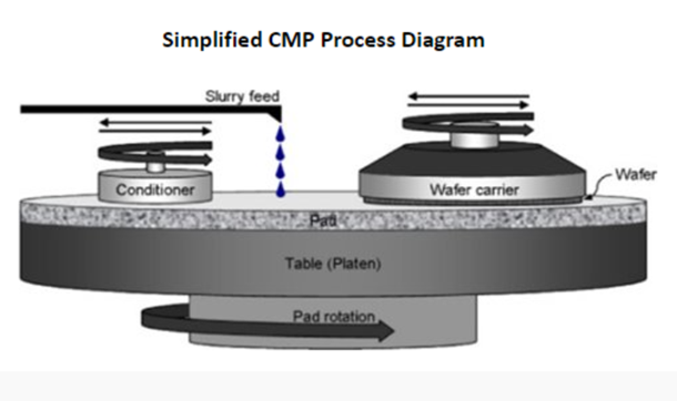
CMP is a method to produce a polished and flat wafer surface. This is necessary since after deposition of materials, the wafer surface is uneven. For subsequent layers, the surface must be planar. The technique involves attaching the wafer with a plastic retaning ring to a metal jig that brings the wafer in contact with an abrasive pad containing a slurry. The pad rotates and with physical and chemical force, the wafer is modified. See the picture below of a simplied CMP process.
[Translate to Japanese:] Arrange technical advice
[Translate to Japanese:]
The performance and service life of plastics for use in the semiconductor industry are influenced by a variety of factors. These criteria need to be considered in order to make the right choice in materials. Examples:
- Antistatic or conductive properties
- Operating temperature
- Contact with chemicals
- Design requirements
- Dimensions and tolerances
- Flame retardancy
We are happy to advise you on the selection of suitable materials for your particular application. Just use our contact form at the bottom of the page.