Select a different country or region to see specific content for your location.
Wafer handling
Materials and solutions for Wafer handling
Materials and solutions for Wafer handling
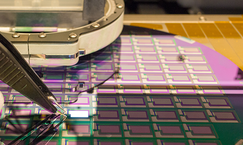
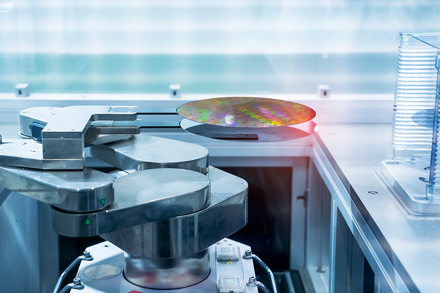
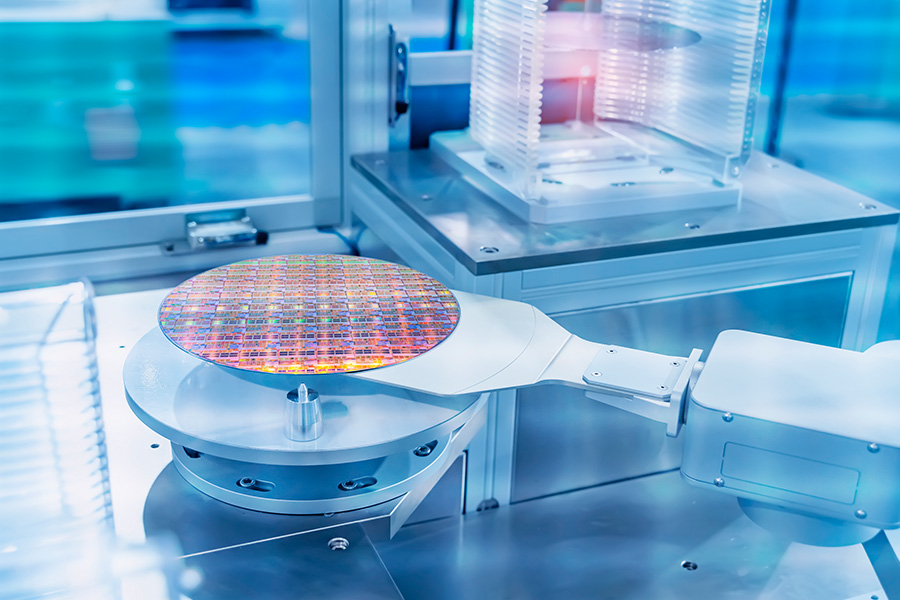
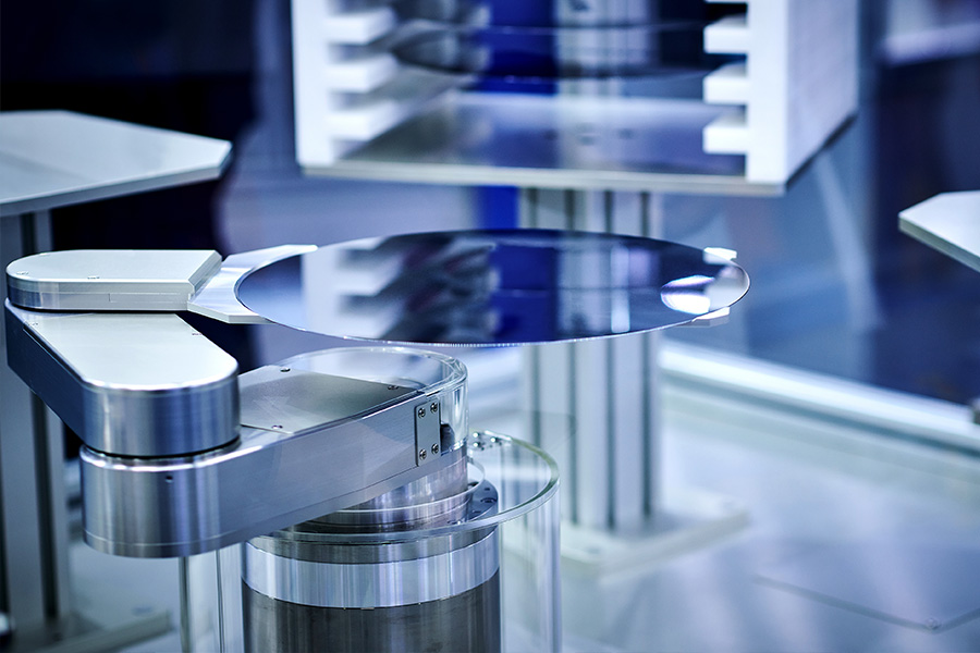
A typical semiconductor factory (fab) includes hundreds of machines that perform a variety of processes for wafer production. Processes include deposition, material removal, patterning, modification of electrical properties, and more. A common element across all these machines is the need for wafer handling tools. These tools include wafer picks/wands, cassettes, FOUPs, grip effectors and automated or robot wafer handlers.
Material properties for Wafer handling:
- Thermal resistance
- Dimensional stability
- Wear resistance
- Outgassing
Typical plastic materials used
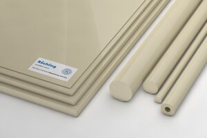
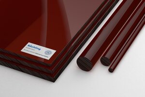
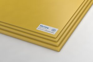
- PEEK reinforced
excellent fatigue and chemical resistance - PEI
high strength and stiffness with good chemical resistance - PVDF
corrosion, acid and alkali resistant - Polyimide
excellent high temperature properties
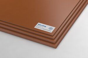
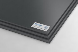
Röchling materials for Wafer handling

Arrange technical advice
The performance and service life of plastics for use in the semiconductor industry are influenced by a variety of factors. These criteria need to be considered in order to make the right choice in materials. Examples:
- Antistatic or conductive properties
- Operating temperature
- Contact with chemicals
- Design requirements
- Dimensions and tolerances
- Flame retardancy
We are happy to advise you on the selection of suitable materials for your particular application. Just use our contact form at the bottom of the page.